Gowin and Andes Team Up on First 22 nm SRAM FPGA With RISC-V Core
FPGA vendor Gowin Semiconductor has teamed with RISC-V IP developer Andes Technology to develop an SRAM FPGA SoC with a hard-instantiated RISC-V core.
RISC-V developers can now take full advantage of FPGA system-on-a-chip (SoC) capabilities by introducing the GW5AST-138 from Gowin Semiconductor. The just-announced SoC contains a hard-instantiated, 32-bit RISC-V core from Andes Technology and a 138K LUT4 SRAM FPGA.

High-end FPGAs have long had Arm cores hard embedded. Now the first 22 nm SRAM FPGA is available with the open-source RISC-V core. Image used courtesy of Andes Technology
One of the many important features of high-performance field programmable gate arrays (FPGAs) is the ability to "instantiate," or create an individual circuit (in this case, a CPU), within the fabric of the FPGA. This allows FPGA designers to tap into the advantages of a processor and execute code for applications better suited to software than hardware. Even better, it allows the FPGA user to utilize both software and custom hardware within the same chip.
Hard-Instantiated CPU Cores Add High-Performance Flexibility
In recent years high-end FPGA vendors have started including CPU cores in hard silicon (a hard core) along with the FPGA. By doing so, a designer can develop a software/custom hardware solution that runs software faster than a soft-instantiated CPU and does not use up valuable FPGA gate count. Traditionally, these hard silicon core implementations have been dominated by Arm architecture CPUs. With this announcement, RISC-V is taking a place on that stage.

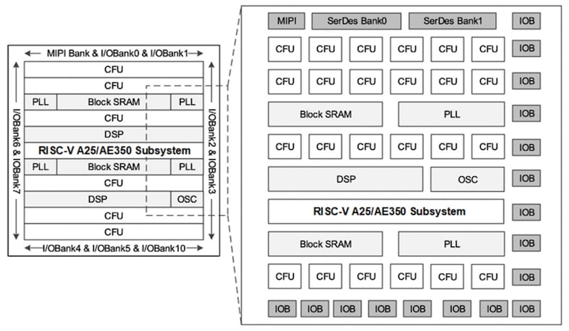
Andes' RISC-V processor architecture implemented in the GW5AST. Image used courtesy of Andes Technology
The GW5AST-138 builds on Gowin’s 22 nm SRAM FPGA architecture and adds the hard-core RISC-V design from Andes. In addition to the CPU, Gowin has added hard instantiations for other major high-performance functional blocks, such as SerDes, Block RAM, DSP, and PCIe interface. By hard instantiating a high-performance CPU and other key functional blocks with the 138K LUT SRAM FPGA, designers can create highly capable systems with minimal external components.
While this is not the first RISC-V hard-instantiated FPGA SoC, it is the first built on an SRAM platform. SRAM FPGAs are volatile and require loading the bitstream from external Flash with each boot. However, they tend to be faster for a given clock speed and have better resistance to single-event errors (SEEs) than Flash FPGAs.
Gowin Leverages Andes' RISC-V Expertise
In 2015, Taiwan-based Andes Technology opened operations in San Jose, California, to develop RISC-V processor core IP. It joined the RISC-V Association as a founding member. To date, Andes has granted more than 200 IP licenses with more than five billion chips shipped.

AndesCore A25 block diagram. Image used courtesy of Andes Technology
The new Gowin SoC includes a 32-bit Andes A25 core running at 400 MHz. It has a RISC-V-compliant ISA with Andes extensions. Some of the key features are:
- DSP/SIMD ISA
- Floating point extensions
- Bit-manipulation extensions
- 32-bit, 5-stage pipelined CPU architecture
- 16/32-bit mixable instruction format
- Memory management unit (MMU) and physical memory protection (PMP)
- Enhanced vectored interrupt handling for real-time performance
The processor supports bare metal and Linux operations.
FPGA Newcomer Gowin Proves Its Mastery
Gowin Semiconductor is a relative newcomer to the FPGA market, having been established in 2014. While Gowin may be young, it has an extensive product line, including many parts that are pin-compatible with Xilinx, Intel, and Lattice Semiconductor parts. Its FPGAs range from as small as 1,152 LUTs up to 138K LUTs, as seen in the GW5AST.
In addition to the hard RISC-V core, the GW5AST includes hard cores for a number of high-performance functions. It includes a hard DSP, PCIe, and MIPI PHY. Key specs for the part are:
- 138K LUT4s
- Block SRAM with multiple modes
- Hardcore DSP with 48-bit accumulator and 12x12, 27x36, 27x18-bit multiplier modes
- Up to 16 global clocks, 6/12 high-performance PLLs, and 16/24 high-speed edge clocks
- SERDES interface at 270 Mbps; 12.5 Gbps operation
- PCI 2.0 hard core supporting x1, x2, x4, x8 lanes
Gowin licenses the development toolchain at no cost. More information is available in the GW5AST datasheet.
More Soft- and Hard-Core SoCs for RISC-V to Come
At the time of this writing, the only other RISC-V hard-core FPGA SoC on the market is Microchip's PolarFire SoC. The PolarFire is a flash FPGA, which means that it is non-volatile and can have near-instant start-up. The PolarFire product line was initially announced in 2018 and has multiple products in the line.
The RISC-V Association includes FPGA veterans Intel (Altera), Xilinx/AMD, Microchip (Microsemi), and Lattice Semiconductor. With all of the major FPGA players in the alliance, designers can expect to see more SoC support for RISC-V, both with soft cores and hard cores.
The practice of embedding hard-core CPUs in an FPGA SoC allows for smaller, high-performance designs in a wide variety of markets. They are especially useful in the automotive, industrial control, and medical markets.


